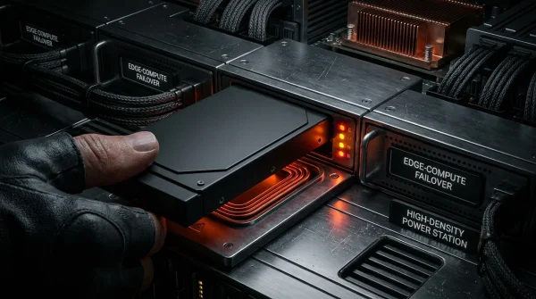
Step inside an enterprise server room in northern Virginia, and the first sensation isn’t the flashing lights of rack-mounted gear; it is the physical push of heat against your chest and the industrial scream of high-RPM blowers forcing chilled air through silicon fins. These server bays run hot enough to bake bread, drawing megawatts just to translate human prompts into probability matrices. For years, you have been told that this roaring, power-hungry sprawl of general-purpose graphics processors is the only road forward.
Every generative model running today—from daily workplace chat tools to massive code generators—relies on an architectural compromise. You rely on chips originally designed to render video game lighting and geometric triangles, retrofitted with matrix math cores to handle natural language.
Because those chips remain general-purpose machines, they spend an enormous portion of their thermal headroom and memory bandwidth juggling speculative tasks, memory caching layers, and software scheduling overhead. They are brilliant Swiss Army knives, but they waste immense amounts of current just keeping their non-relevant circuitry awake. When you watch enterprise budgets strain under seven-figure hardware leasing costs, you are witnessing the physical limit of asking a generalist to do a specialist’s job.
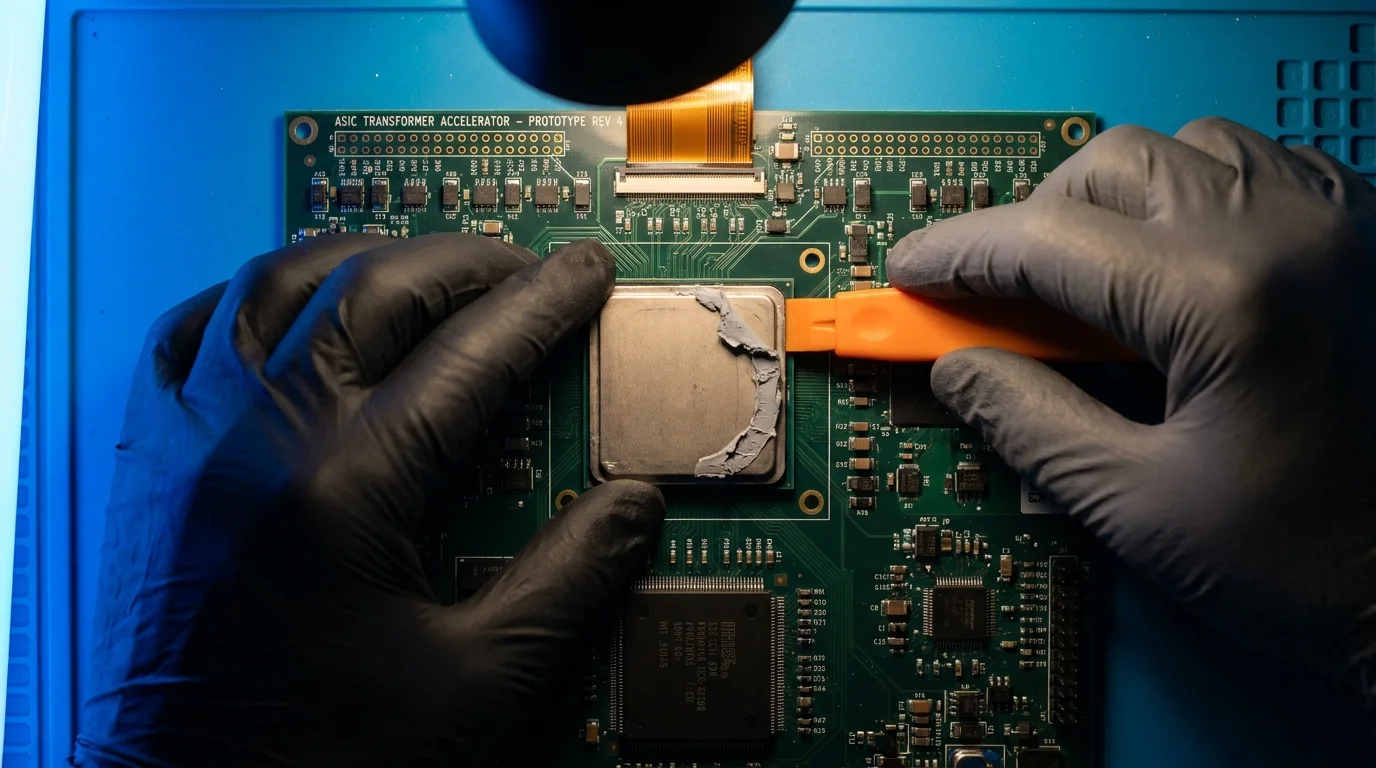
Now, a radical bet out of Silicon Valley is rewriting that calculation, etching the transformer algorithm directly into raw silicon and stripping away every single logic gate that does not serve attention mechanisms.
The Fallacy of the Universal Processor
For two decades, modern computing lived by an unwritten contract: software changes continuously, so your underlying silicon must remain fluid. If a developer invents a new neural network topology tomorrow, a flexible graphics processor can adjust via a routine driver update. But that flexibility extracts a devastating tax on throughput.
Imagine hiring a master cabinetmaker to mass-produce identical cedar dowels, only for him to spend forty minutes sharpening six different chisels before cutting a single piece. An Application-Specific Integrated Circuit, or ASIC, throws away the toolbox. It is not an adaptable workshop; it is an automated die press that stamps out the exact shape you need with zero mechanical waste. By physically hardwiring the mathematical operations of transformer attention mechanisms—specifically the key, query, and value matrix multiplications—straight onto the die, specialized chips discard instruction decoders, graphics pipelines, and dynamic scheduling circuits.
- Temu mobile app updates silently restore clipboard tracking behind muted privacy alerts
- iPhone 16 Pro haptic motors trigger phantom leg buzzes during quiet desk hours
- Samsung Galaxy S23 firmware silently caps processor speeds behind scalding glass backs
- Salesforce cloud servers crash nationwide leaving thousands of mobile business teams disconnected
- iPhone 14 battery replacements defeat pricey flagship upgrades reviving drained battery bars
The result is startling in its simplicity. When you strip out the circuitry needed to run physics engines or varied neural network structures like convolutional nets, you free up massive surface area on the wafer. That freed silicon real estate goes directly toward raw compute density and ultra-wide memory buses, allowing tokens to stream out without waiting on memory queue bottlenecks.
The Kitchen-Table Architecture
Consider Marcus Vance, a 44-year-old high-performance infrastructure architect who spent fifteen years outfitting enterprise financial firms with dense compute clusters. Last autumn, while auditing power consumption at a Phoenix colocation facility, Marcus realized his team was spending 42% of their electrical budget simply shuffling weights between separate high-bandwidth memory stacks and processor cores. The silicon wasn’t computing; it was waiting in line at the buffet.
When startups like Etched surfaced with tens of millions in venture capital backing to build their flagship processor, Sohu, they targeted precisely that friction point. Instead of trying to run every machine learning flavor under the sun, they burned the transformer architecture into the physical gates. By betting their entire balance sheet on one mathematical framework, they eliminated the traditional software-translation barrier, driving latency down to the hard physics of electron travel across copper interconnects.
Infrastructure Layers: Mapping Your Workload Strategy
Adopting specialized silicon over industry-standard server clusters isn’t an all-or-nothing proposition. It demands looking at your software pipelines through the lens of longevity versus experimentation.
For the Enterprise Scale-Out
If your organization runs millions of inference queries daily against stable foundation models, standard generalist hardware is actively siphoning your capital. Fixed-architecture chips allow you to run massive batch sizes at a fraction of the thermal footprint, turning warehouse-scale power limitations into sustainable continuous throughput.
For the Frontier Researcher
If your team spends its weeks experimenting with non-transformer architectures, state-space models, or exotic recurrent mechanisms, hardware ASICs are not your sanctuary. A hardwired transformer chip cannot adapt if you throw away the self-attention formula; its greatest strength—immutability—becomes a dead-end brick if your model abandons attention altogether.
For the Lean Platform Builder
Platform operators serving customer-facing applications live and die by latency to first token. When you run inference on dedicated silicon, you bypass the kernel launch latency and driver overhead that plague mainstream graphics accelerators, letting you deliver conversational responses with the immediacy of local hardware.
The Mindful Deployment Sequence
Transitioning enterprise infrastructure toward specialized ASIC environments requires a measured, diagnostic touch. You do not tear down existing racks overnight; you systematically peel away fixed inference workloads.
- Profile your compute distribution: Audit your cluster logs over a 90-day window to determine the exact percentage of compute spent on training versus production inference.
- Isolate stable transformer weights: Identify production models whose core attention architectures have remained stable across your last two release cycles.
- Calculate the thermal coefficient: Measure the true cost per generated million tokens, including cooling and facility power distribution losses, rather than relying on chip manufacturer peak TFLOPS.
- Benchmark latency floors: Run small-batch queries through specialized hardware emulators to verify that memory bandwidth matches your real-world concurrency needs.
Keep these baseline parameters in focus: target inference operating temperatures between 140°F and 160°F to prevent thermal throttling; maintain a memory bandwidth floor of at least 3.0 TB/s per rack unit; and verify that host-to-accelerator interconnect latency stays strictly below 5 microseconds.
The Quiet Power of Singular Purpose
In an industry obsessed with speculative versatility, there is profound quietude in doing one thing with uncompromising precision. The frenzy to secure warehouse allotments of general-purpose cards has created an artificial scarcity, convincing teams that more raw watts and larger fan arrays are the only solutions to scaling bottlenecks.
When you strip away the digital clutter—the legacy instruction sets, the unused registers, the layers of driver virtualization—you uncover a cleaner relationship with compute. The emergence of purpose-built silicon reminds us that progress is not always about building a machine that can solve every imaginable puzzle. Sometimes, true technical mastery means forging an instrument that does precisely what you need, with absolute clarity, and not a single wasted spark.
Specialized silicon turns structural mathematical certainty into raw physical efficiency, leaving generalized bloat behind.
| Key Point | Detail | Added Value for the Reader |
|---|---|---|
| Architecture Focus | Hardwired transformer attention layers versus general-purpose parallel compute pipelines. | Eliminates unnecessary logic gates to maximize power and thermal efficiency. |
| Memory Access | Direct on-chip datapath routing that reduces external memory latency spikes. | Dramatically lowers time-to-first-token for real-time user experiences. |
| Operational Risk | Rigid hardware specificity that cannot run non-transformer algorithmic topologies. | Protects capital expenditure by matching purchase strategy strictly to stable production models. |
Frequently Asked Questions
What happens if modern AI models evolve away from transformer architectures?
If the fundamental mathematics shift away from attention mechanisms, hardwired ASICs cannot adapt and would require redesigning new silicon dies from scratch.Why haven’t existing market leaders focused exclusively on transformer-only chips?
Incumbents serve diverse markets including scientific simulation, graphics rendering, and experimental research, requiring them to maintain broad software and hardware flexibility.Does ASIC hardware replace the need for traditional training clusters?
No, these specialized chips are primarily engineered to dominate enterprise inference, where models are deployed at scale after initial training on adaptable hardware.How does this impact localized data center power consumption?
By cutting out extraneous compute pipelines, specialized silicon delivers substantially higher throughput per watt, directly lowering cooling and energy overhead.Can small development teams take advantage of this hardware shift?
Yes, as cloud hosting providers adopt specialized silicon racks, smaller teams will access significantly cheaper API-driven inference rates without buying the physical hardware.