Step onto the raised floor of an enterprise data hall, and you will hear a distinct mechanical roar. Chillers push air conditioned to sixty degrees Fahrenheit through perforated floor tiles, fighting a continuous war against heat. In standard server racks, thousands of modest, thumb-sized silicon dies sit separated by inches of fiberglass board, copper traces, and optical transceivers.
We have spent decades accepting a strange logistical compromise. We slice circular silicon ingots into neat little squares, throw away the edges, test each die for flaws, and then spend millions of dollars trying to make those separated chips communicate through microscopic external wires. It is like building an entire metropolitan workforce, housing them in separate towns, and forcing them to collaborate through a single one-lane toll bridge.
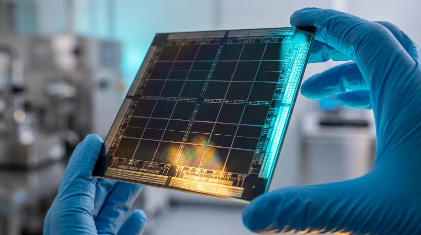
When you look closely at Cerebras Systems hardware, that familiar compromise evaporates. What sits in their rack is not a conventional package, but a giant, uncut, plate-sized monolithic slab of silicon. By skipping the traditional dicing stage entirely, this wafer-scale architecture treats an entire 300-millimeter circular wafer as one continuous computing canvas.
The result reshapes how neural weights move across hardware. Instead of letting memory travel yards across printed circuit boards, data travels millimeters across bare silicon, cutting latency down to negligible whispers.
The Silicon Cookie Cutter: Reimagining the Wafer Bottleneck
For fifty years, semiconductor manufacturing followed a predictable, defensive doctrine. Foundries expected microscopic chemical imperfections on every silicon disc. Because a single stray speck of dust could ruin a circuit, fabricators cut the disc into hundreds of small chips, discarding the duds and keeping the functional survivors.
This defensive manufacturing strategy created an artificial wall known as the reticle limit. Traditional lithography machines can only print a pattern roughly twenty-six by thirty-three millimeters wide. When an artificial intelligence model outgrows that perimeter, engineers have to stitch multiple separate chips together across circuit boards, where communication speeds drop by a factor of thousands.
Cerebras bypassed this limitation not by making pristine silicon without flaws, but by engineering built-in redundancy directly into the fabric. They etch identical compute cores across the wafer surface and link them with an intelligent crossbar network. If a dust grain ruins twenty cores on a wafer, the system simply routes around those dead spots at the silicon level, leaving hundreds of thousands of neighboring cores completely intact and connected.
- Facebook Messenger updates quietly reactivate clipboard snooping behind dimmed smartphone screens
- Smartphone vibration motors trigger false pocket buzzes while resting on distant wooden desks
- Dell XPS laptops quietly cap processor clock speeds behind scorching hot metal keyboards
- Smartphone market carriers switch 5G midband frequencies dropping legacy rural cellular roaming
- AMD Radeon drivers block zero-day desktop exploits following urgent consumer security update
Instead of chopping the wafer into islands and trying to bridge the ocean, Cerebras kept the continent whole. The silicon stays unbroken, and the data never needs to convert its electrical language into bus protocols or fiber-optic signals.
The Field Reality: Elena Vance on Interconnect Friction
Elena Vance, a forty-two-year-old distributed systems engineer in Austin, spent years trying to scale frontier language models across clusters of standard graphics cards. Her workdays were not spent improving neural weights; they were spent diagnosing networking dropouts and packet serialization delays.
“In traditional clusters, you spend eighty percent of your engineering time fighting the network,” Vance explains. “You have to break your model into shards, balance pipeline stages, and pray that an optical transceiver doesn’t overheat mid-epoch. When you run a workload across an entire unbroken wafer, the concept of distributed memory synchronization almost vanishes. The model fits entirely on the silicon, and training feels like writing code for a single machine again.”
Workload Segmentation: Matching Tasks to the Wafer
Wafer-scale compute alters how different computing environments manage large-scale deep learning models. Depending on your operational bottlenecks, the hardware delivers distinct architectural shifts.
For Real-Time Inference Pipelines: Conventional accelerators depend on off-chip graphics memory (HBM), which throttles performance when serving single-token queries to millions of users. Because wafer-scale engines keep all memory directly on-chip, memory bandwidth constraints disappear entirely, allowing teams to deliver instant conversational feedback without batching requests.
For Massive Parameter Training: Sharding a multi-billion-parameter network across dozens of traditional server nodes requires complex distributed frameworks and manual tensor partitioning. On an uncut wafer, the entire parameter state resides in a unified memory fabric, stripping away the software overhead of distributed parallelism.
For Research Labs Under Space Constraints: A traditional compute cluster consuming forty racks of hardware demands complex cooling loops, miles of fragile cabling, and dedicated networking switches. Consolidating that compute into a compact footprint simplifies power delivery and slashes the physical failure points of multi-node networking.
Mindful Architecture: The Tactical Silicon Toolkit
Operating a piece of hardware that consumes twenty kilowatts across a single sheet of silicon requires an uncompromising approach to physics. You cannot cool a wafer using simple copper fins and spinning fans; the heat density demands direct liquid contact.
Cerebras solves this using an internal liquid cooling manifold that pumps water directly across the back of the silicon sheet. The copper cold plate acts like an artificial circulatory system, balancing temperatures across the entire surface.
- Transistor Scale: Over four trillion transistors unified on a single engine, compared to roughly eighty billion on conventional flagship accelerators.
- Core Density: Nine hundred thousand AI-optimized cores operating synchronously on a single physical wafer.
- On-Chip Storage: Forty-four gigabytes of ultra-fast static RAM (SRAM) woven directly next to arithmetic units.
- Fabric Throughput: Twenty-one petabytes per second of internal bandwidth, outperforming board-level interconnects by several orders of magnitude.
- Thermal Thresholds: Maintained via internal liquid manifolds operating at precise pressure metrics to prevent thermal gradients across the silicon plane.
By bringing memory directly to the arithmetic logic gates, the machine avoids the energy-hungry task of shuttling bits back and forth over external buses. Compute becomes cool, focused, and immediate.
Beyond the Packaging Trap
When you step back from the raw benchmark numbers, the arrival of working wafer-scale systems proves that industry dogmas are often just habits dressed up as physical laws. We spent decades assuming that chips had to be small because factories were imperfect. We accepted the friction of slow cables and fragmented memory because that was simply how computers had always been put together.
By learning to live with manufacturing flaws rather than running from them, engineers built something that feels less like an assembly of spare parts and more like a singular, living organism. It reminds us that real progress does not always come from polishing existing limits. Sometimes, you just stop cutting the wafer.
The fastest communication link between two transistors is the one that never leaves the surface of the silicon.
| Key Point | Detail | Added Value for the Reader |
|---|---|---|
| Manufacturing Logic | Replaces wafer dicing with fault-tolerant redundancy routing. | Explains how hardware survives manufacturing defects without sacrificing performance. |
| Memory Access | Eliminates off-chip HBM bottlenecks using massive on-chip SRAM. | Demonstrates why models run without memory-bandwidth starvation. |
| System Simplicity | Replaces miles of cluster networking cables with on-silicon crossbars. | Reduces cluster debugging complexity and hardware point-of-failure risks. |
Frequently Asked Questions
How does Cerebras deal with manufacturing defects on such a large chip?
The system includes redundant processing cores and bypass interconnects. If a manufacturing defect occurs at a specific point on the wafer, the system software simply routes traffic around the inactive core without affecting the rest of the fabric.Why don't conventional chipmakers build wafer-scale hardware?
Traditional foundries maximize profit by selling individual, high-yielding dies for diverse markets. Wafer-scale hardware requires proprietary liquid-cooling distribution, specialized power delivery systems, and bespoke packaging techniques that deviate from standard consumer manufacturing lines.Does wafer-scale hardware replace standard data center clusters?
It complements them for specific high-intensity workloads. While standard clusters remain ideal for diverse, multi-tenant cloud tasks, wafer-scale engines excel at giant deep-learning workloads that otherwise choke on network communication.How is a giant single-wafer chip kept cool?
It uses a custom liquid-cooling manifold that sits flush against the silicon. Chilled liquid flows directly across the cooling plate to pull heat away evenly, preventing hot spots from warping the material.What is the primary operational benefit for AI developers?
Simplicity in model execution. Instead of dividing neural networks across thousands of small GPUs using complex pipeline parallelism, developers can compile large models onto a unified architecture with minimal distributed code overhead.